Article

Excited States Calculations of MoS2@ZnO and WS2@ZnO Two-Dimensional Nanocomposites for Water-Splitting Applications

1
Institute of Solid State Physics, University of Latvia, 8 Kengaraga str., LV-1063 Riga, Latvia
2
Transport and Telecommunication Institute, LV-1019 Riga, Latvia
*
Author to whom correspondence should be addressed.
Energies 2022, 15(1), 150; https://doi.org/10.3390/en15010150
Submission received: 29 November 2021 / Revised: 23 December 2021 / Accepted: 23 December 2021 / Published: 27 December 2021

Abstract

:
Transition metal dichalcogenide (TMD) MoS 2 and WS 2 monolayers (MLs) deposited atop of crystalline zinc oxide (ZnO) and graphene-like ZnO (g-ZnO) substrates have been investigated by means of density functional theory (DFT) using PBE and GLLBSC exchange-correlation functionals. In this work, the electronic structure and optical properties of studied hybrid nanomaterials are described in view of the influence of ZnO substrates thickness on the MoS 2 @ZnO and WS 2 @ZnO two-dimensional (2D) nanocomposites. The thicker ZnO substrate not only triggers the decrease of the imaginary part of dielectric function relatively to more thinner g-ZnO but also results in the less accumulated charge density in the vicinity of the Mo and W atoms at the conduction band minimum. Based on the results of our calculations, we predict that MoS 2 and WS 2 monolayers placed at g-ZnO substrate yield essential enhancement of the photoabsorption in the visible region of solar spectra and, thus, can be used as a promising catalyst for photo-driven water splitting applications.

1. Introduction

Zinc oxide (ZnO), one of the potential photocatalysts for water-splitting applications, has been extensively studied at nanoscale for photocatalysis [1], photosensorics [2,3,4,5], and for other industrial applications [6,7,8,9,10,11,12,13], including energy generation by transformation of waste heat energy to electricity through thermoelectric power generation using Al-doped ZnO nanostructures [14,15].
From the viewpoint of solar spectra utilization, the band gap of ZnO (3.3∼3.4 eV) allows for harvesting solar radiation only in the UV region [16,17,18]. In addition, the direct band gap of ZnO crystalline materials leads to rapid recombination of photogenerated electron-hole pairs, which restricts its efficient usage as a photocatalyst [19]. Recently, the layered TMDs have been studied due to their excellent catalytic and optical characteristics [20,21]. Synthesis of WS 2 @ZnO and MoS 2 @ZnO core-shell nanowires with TMD shell thickness down to a few monolayers was reported by us elsewhere [22,23]. TMD coatings were produced from WO 3 or MoO 3 thin layers deposited by magnetron sputtering on ZnO nanowires and annealed in a sulfur atmosphere. It has been shown that combining the TMD materials with other wide-gap semiconductors could not only increase their broadband photoresponse but also enhance their absorption in the visible region of solar spectra [3,4,22,23,24].
Recent theoretical investigations [25,26,27,28,29,30] confirm that the heterostructures made of ZnO ML and TMD ML can actually enhance photon absorption under visible light irradiation. There is also a distinct interest in industrial use of MX 2 @ZnO heterostructures for applications towards environmental remediation and photocatalytic degradation of methyl blue [31,32]. A series of MX 2 @ZnO (M = Mo, W; X = S, Se) heterostructures were suggested as materials with enhanced photoabsorption in the visible light region. Efficient photocatalyst for hydrogen production in water-splitting should possess the valence band maximum (VBM) located below the energy of thermodynamically favorable oxygen reduction reaction (–5.67 eV with respect to the vacuum level) [33], while its conduction band minimum (CBM) should be located above the standard hydrogen electrode (SHE, –4.44 eV with respect to the vacuum level). MS 2 ML (M = Mo, W) placed at ZnO ML meets these two requirements [26,27].
It is necessary to emphasize that to take into account all processes taking place during optical excitation is not an easy task, on the one hand, and, on the other, to perform reliable theoretical predictions, they have to be included into calculations, at least to some extent. In this study, we have analyzed the photocatalytic properties taking into account the photon excitations. In addition to photocatalysis [2,3], excited states calculations are important for the description of various processes in photostimulated desorption from the solid surfaces [34], photostimulated diffusion and photoinduced transformations of point defects under excitations [35,36,37,38,39], photo-induced exciton relaxation with defect formation [40], and processes of optical storage and optically stimulated luminescence [38,41,42].
To take into account excitation effect in this work, the MoS 2 @ZnO and WS 2 @ZnO 2D nanocomposites are theoretically studied using DFT (including excited-state time-independent DFT). Constructed heterostructures consist of TMD monolayer deposited atop of 1-, 2-, and 4-layered ZnO substrate. (The 1-, 2-, and 4-layered ZnO structures are hereafter denoted as 1ML-ZnO, 2ML-ZnO, and 4ML-ZnO, respectively.) In 2005, Claeyssens et al. theoretically predicted the structural transition of ZnO thin films from the wurtzite phase to the graphene-like ZnO phase (g-ZnO) for nanofilms thinner than 18 atomic layers (9 ML) [43]. The stable g-ZnO structure was experimentally observed in 2007. Tusche et al. reported that the transformation to g-ZnO takes place if a ZnO thin film contains 3–4 ML [44]. It was found that the length of Zn–O chemical bond in the planes of g-ZnO honeycomb structure is shorter than in the wurtzite ZnO (w-ZnO) bulk phase. The length of the Zn–O bond between different layers in g-ZnO is about ∼11% larger than in its wurtzite phase [44,45]. In this study, the 1ML-ZnO and 2ML-ZnO models were constructed to mimic the g-ZnO; in turn, 4ML-ZnO mimics w-ZnO thin films.
We have calculated from the first principles the electronic structure and optical properties of MoS 2 and WS 2 ML deposited atop free-standing 1ML-ZnO, as well 2ML-ZnO and 4ML-ZnO substrates. Based on data available in the literature [25,26,27,29], one knows that the monolayered ZnO combined with MoS 2 or WS 2 ML, irrespective of mutual layer orientation, keeps the constant band gap, as well as fulfills the condition of band edge alignment with respect to the water splitting redox levels. Taking this into account, in our study, we have chosen two configurations of ZnO substrate orientation relative to MoS 2 and WS 2 ML, with the rotation angle of 0 and 180 , as it is described in Refs. [26,27] (see the “Computational Details and Models of Heterostructured” section for detailed explanation of the model). The electronic band structure and projected density of states (PDOS) of free-standing 1ML-ZnO, 2ML-ZnO, and 4ML-ZnO substrates, and free-standing MoS 2 and WS 2 MLs, as well as of MoS 2 @ZnO and WS 2 @ZnO nanocomposites, were calculated by means of DFT. The dependence of optical absorption of MoS 2 @ZnO and MoS 2 @ZnO 2D nanocomposites upon the thickness of ZnO substrate is estimated through the calculated frequency-dependent dielectric function. The excited states calculations are used to obtain transition states of photogenerated electrons in nanocomposites under study. A brief summary and conclusions on photocatalytic properties of studied heterostructures are given at the end of this paper.

2. Computational Details and Models of Heterostructures

All first principle simulations reported in this paper were performed using the GPAW computer code [46,47] and ASE library [48,49]. The electronic configurations of valence electrons were adopted as follows: O(2s 2 2p 4 ), Zn(3d 10 4s 2 ), S(3s 2 3p 4 ), W(5p 6 6s 2 5d 4 ), and Mo(4p 6 4d 5 5s 1 ). The geometry relaxation has been obtained by means of Broyden-Fletcher-Goldfarb-Shanno (BFGS) algorithm within the frameworks of Perdew-Burke-Ernzerhof (PBE) exchange-correlation functional (E X C ) [50]. Further optimization of atomic coordinates was carried out to reach their equilibrium positions using DFT-D3 correction of Grimme [51] that considers weak dispersion forces. To calculate the electronic structure, the PBE and the Gritsenko-van Leeuwen-van Lenthe-Baerends with the solid-state modification (GLLBSC) [52] E X C s were used. To overcome underestimation of ZnO band gap, the Hubbard DFT+U scheme [53] was used to describe the localized electrons. Hubbard potentials U d , Z n = 10 eV and U p , O = 7 eV are adopted for our calculations [16,54]. We note that, though the selected U d , Z n and U p , O for the ZnO bulk phase predict reliable band gap, the Hubbard correction for localized Zn d-state results in the underestimated lattice parameters, caused by the increasing interaction force between electrons and the core [16,54].
The energy cutoff for the plane-wave basis expansion was chosen to be 500 eV. The convergence accuracy of energy and atomic force are set to 10 5 eV and 0.05 eV/Å, respectively. For the Brillouin zone integration, the 6 × 6 × 1 k-points mesh was used. A 12 Å-thick vacuum gap was added to avoid the interaction of periodically repeated slabs of studied materials. The models adopted for MoS 2 @ZnO and WS 2 @ZnO 2D nanocomposites consist of 2 × 2 surface supercell (SC) for 1ML-ZnO, 2ML-ZnO graphene-like, and 4ML-ZnO wurtzite-like substrates with 2 × 2 surface SC of MoS 2 and WS 2 MLs attached to them (Figure 1). Calculated lattice mismatch in MoS 2 @g-ZnO, WS 2 @g-ZnO, MoS 2 @w-ZnO, and WS 2 @w-ZnO are 1.88, 1.91, 0.02, and 0.05 %, respectively. In fact, it makes an epitaxial growth of MoS 2 @ZnO and WS 2 @ZnO 2D nanocomposites possible. Calculated Mo–S bond length of 2.411 Å is in good agreement with the bond length of 2.413 Å reported by Wang et al. [27], while calculated W–S bond length of 2.420 Å coincides with the one reported by Guan et al. [55].
The TMD ML placed atop of g-ZnO substrate is known to be sensitive to the mutual rotation of the TMD ML and ZnO nanofilm relative to each other. The rotation angles may not only cause the changes of band gap values but also may shift the VBM/CBM with respect to the water splitting redox level [26,27]. However, there are no significant indications of the band gap and band edge positions changes in respect to the rotation angles for MoS 2 @ZnO and WS 2 @ZnO 2D nanocomposites studied here. This study is mainly focused on the optical properties, especially on the influence of ZnO substrate thickness to optical properties of MoS 2 @ZnO and WS 2 @ZnO nanocomposites. That is why we have limited ourselves to calculations of the models with rotation angles of 0 and 180 . The models of MoS 2 @ZnO and WS 2 @ZnO nanocomposites used in our calculations are shown in Figure 1. In order to correctly reproduce graphene-like 2ML-ZnO substrate, as well as wurtzite-like 4ML-ZnO substrate, these models were relaxed with the fixed Zn atoms. For 1ML-ZnO substrate, the complete geometry optimization without any restrictions was performed. After the MoS 2 and WS 2 MLs attached to the ZnO substrates, the heterostructures were relaxed with the fixed O atoms. The fixed lattice constants are used here to avoid the strain [26,27]. The positions of the band edges with respect to the vacuum level were computed by averaging the slab electrostatic potential which was performed by solving the Poisson equation from the pseudo charge at the ground state.
To predict optical properties, the linear density response approach within the framework of projector-augmented wave method [56] was applied to calculate the frequency-dependent dielectric function ε ( ω ) = ε 1 ( ω ) + j ε 2 ( ω ) of the free-standing ZnO substrates, free-standing MoS 2 and WS 2 MLs, and MoS 2 @ZnO and WS 2 @ZnO nanocomposites. ε 1 and ε 2 are the real and imaginary part of the complex dielectric function, respectively.
The plane wave cutoff energy to define the dielectric matrix was set to 80 eV, the frequency grid was set to 0.05 eV. For the free-standing MoS 2 ML and WS 2 ML, the Bethe-Salpeter equation (BSE) was used to calculate the dielectric function with the excitonic effects [56,57,58]. To calculate the total charge density of excited states the non-Aufbau orbital occupation approach was used to solve the excited-state self-consistent field equation [59]. To avoid numerical collapse, we used the maximum overlap method (MOM) [60,61]. VESTA software package [62] was used to visualize the nanostructures under study. Python packages NumPy [63] and Matplotlib [64] were used to analyze the calculated data and to produce figures.

3. Results and Discussion

3.1. Pristine ZnO, MoS 2 , and WS 2

Figure 2 schematically shows both non-distorted and equilibrium atomic structures of ZnO substrates.
Analyzing optimized geometries of 1ML-ZnO and 2ML-ZnO substrates, they clearly possess a graphene-like ZnO structure with no obvious bonds formed between layers. In contrast, the 4ML-ZnO preserves the crystal symmetry of wurtzite ZnO and, further on, is adopted in this study to mimic the wurtzite-like ZnO substrate. The calculated lattice constant for ZnO bulk is 3.050 Å. Though the lattice constant of ZnO bulk agrees well with the value predicted elsewhere (3.052 Å) [16,54], optimized lattice parameters by means of the DFT+U are underestimated compared to 3.25 Å obtained in the experiments and predicted by simulation without the Hubbard corrections [16,25,26,27,29,54]. In the literature, it is reported that the Zn–O bond length between pseudo-planes in the w-ZnO (d’ Z n O ) is 2.14–2.16 Å [43,44]. In our 4ML-ZnO model, the d’ Z n O in 1–2 ML planes and 2–3 ML planes are 2.172 and 2.155 Å, respectively. Calculated lattice constant for 4ML-ZnO substrate is around 6.3% underestimate the lattice constant published elsewhere [54] and is in a good agreement with other theoretical predictions [43] and experimental measurements [44].
Figure 3 shows the atomic structure and the band gap of free-standing ZnO and g-ZnO substrates, as well as the frequency-dependent imaginary part of dielectric function ( ε 2 ) calculated for them. The calculated band gap of 1ML-ZnO, 2ML-ZnO, 4ML-ZnO, and ZnO bulk using PBE and GLLBSC E X C s is shown in Figure 3a. As the thickness of the ZnO substrate is increased, the band gap approaches the ZnO bulk value. Due to the strong quantum confinement effect, our calculations predict a larger band gap for the free-standing 1ML-ZnO and 2ML-ZnO, in agreement with recent experimental observations [65]. Our calculations reveal that 1ML-ZnO, 2ML-ZnO (g-ZnO), and 4ML-ZnO (w-ZnO) are direct band gap semiconductors with the VBM and CBM located at the Γ point. The GLLBSC E X C predicts the band gap of bulk ZnO closer to that experimentally observed (3.3–3.4 eV) [66]. The bulk ZnO band gap calculated with PBE E X C (2.49 eV) is underestimated with respect to the value predicted elsewhere by means of HSE06 E X C (3.29 eV [25,26,27,29]) and G0W0 approach (3.57 eV [67]), as well. Calculations performed by means of PBE E X C (classical GGA DFT) are shown here for comparative purposes. From the experiment [68], one knows that the gradually thinner ZnO thin films reveal not only reduced ε 2 but also produce the slightly blue-shifted main peaks in the vicinity of 3.4 eV (365 nm).
To estimate optical response, the ε 2 calculated for 1ML-ZnO, 2ML-ZnO, and 4ML-ZnO substrates are presented in Figure 3b. Layered ZnO substrates calculated with GLLBSC E X C yield the blue-shifted spectra with respect to those calculated using PBE E X C , which underestimates the ZnO band gap. The ε 2 of the 2ML-ZnO calculated with both PBE and GLLBSC E X C is more blue-shifted in comparison with 1ML- and 4ML-ZnO. We note that it is reasonable to take into consideration the excitonic effects calculating the dielectric function of van der Waals materials, e.g., BSE method [29,57,58]. In this study, we concentrate on the consequence of w-ZnO and g-ZnO being a substrate for 2D nanocomposites consisting of ZnO and TMDs monolayers, in which optical properties can be obtained without considering the excitonic effect [25,26,27,29].
Band structures and projected density of states (PDOS) calculated for both MoS 2 and WS 2 MLs are shown in Figure 4a,b, respectively. PDOS calculated by means of both PBE and GLLBSC E X C s reveal that the 2 × 2 SC yields more dense Mo and W states in the vicinity of the VBM. The excess of Mo state shifts the VBM from the K point to the Γ point. In addition, the CBM eigenvalue of MoS 2 and WS 2 at K point also decreases. The optimized lattice constant for the MoS 2 and WS 2 are 3.16 and 3.17 Å, respectively. Calculated lattice constants are in a good agreement with those reported elsewhere [25,26,27,29].
The ε 2 calculated for MoS 2 and WS 2 are illustrated in Figure 5. The ground state calculations of TMDs are performed using 2 × 2 SC. The ε 2 is calculated taking into account the excitonic effects and, without it, differs a lot. The ε 2 without the excitonic effects presents the apparent blue-shift [68]. The distinct peaks predicted with the use of excitonic effects have a good agreement with those previously theoretically predicted, as well as with those observed in the experiment [68,69,70]. As compared to the ZnO substrates, the ε 2 calculated for TMDs exhibits stronger absorption in the visible light region. Therefore, it is expected that the 2D nanocomposites made of ZnO and TMDs MLs may lead to enhanced photoresponse.

3.2. Electronic Structure

Positions of the band edge calculated for all 2D nanocomposites under study are related to the water splitting redox levels in Figure 6. Considering the 1ML-ZnO substrate, the band edge positions of MoS 2 @ZnO and WS 2 @ZnO 2D nanocomposites with the rotation angle of 0 and 180 are in good agreement with those reported elsewhere [25,26,27,29]. We note that the choice of exchange-correlation functional affects the band edge positions of studied nanocomposites. On the whole, the GLLBSC calculated VBM and CBM are more reliable with respect to those calculated by means of PBE E X C . MoS 2 @ZnO with 1ML-ZnO and 4ML-ZnO substrate is generally not suitable for spontaneous production of the hydrogen through the photocatalytic water splitting reaction. In contrast, the WS 2 @ZnO 2D nanocomposites fit well to the water splitting redox levels.
To investigate the electronic structure of 2D nanocomposites, the band structures and PDOS of MoS 2 @ZnO and WS 2 @ZnO are shown in Figure 7. The band gap of MoS 2 @1ML-ZnO and WS 2 @1ML-ZnO with the rotation angle of 0 and 180 is around 1.0–1.5 eV, in a good agreement with previously published [25,26,27,29]. Considering the PBE E X C , most of the VBM are occupied by O states at Γ point, except as shown in Figure 7d,j. For these two cases, the interband transition takes place from the Mo (W) VBM at Γ point to Mo (W) CBM at K point instead of the O VBM at Γ point to Mo (W) CBM at Γ point. Conversely, most of the VBM calculated with GLLBSC E X C are dominated by Mo (W) VBM at Γ and K points. This phenomenon results in three types of band gap predicted by GLLBSC. First, most cases of the band gap are the indirect band gap from Mo (W) VBM at Γ point to Mo (W) CBM at K point, as shown in Figure 7a,d,e,g,i,j. Second, as originally expected, the transition occurs from O VBM at Γ point to Mo (W) CBM at K point, as shown in Figure 7b,c,f. Third, the indirect band gap becomes the direct one with the transition from Mo (W) VBM to CBM at K point in Figure 7h,k,l.
Due to underestimated band gap, the CBM obtained by means of PBE E X C is always laying deeper than the one calculated by means of GLLBSC. For all the nanocomposites under study, the CBM is determined by the Mo and W states. On the contrary, the VBM is predicted differently by PBE and GLLBSC E X C s. The valence bands close to VBM calculated with the PBE consist of the O 2 p states. As the ZnO substrate becomes thicker, more dense O states are accumulated at Γ and K point. PBE mostly predicts the indirect band gap with the VBM at Γ and CBM at K point. For the g-ZnO substrates, the density of states around the VBM mainly consists of transition metal orbitals. Even if the 4ML-ZnO substrate provides abundant O states, the Mo (W) orbitals still have a tremendous effect compared to the prediction made by PBE calculations. It is also worth mentioning that the GLLBSC E X C always predicts the valence band consisting of Mo and W orbitals around VBM at K point and, thus, yields the direct band gap.

3.3. Optical Properties

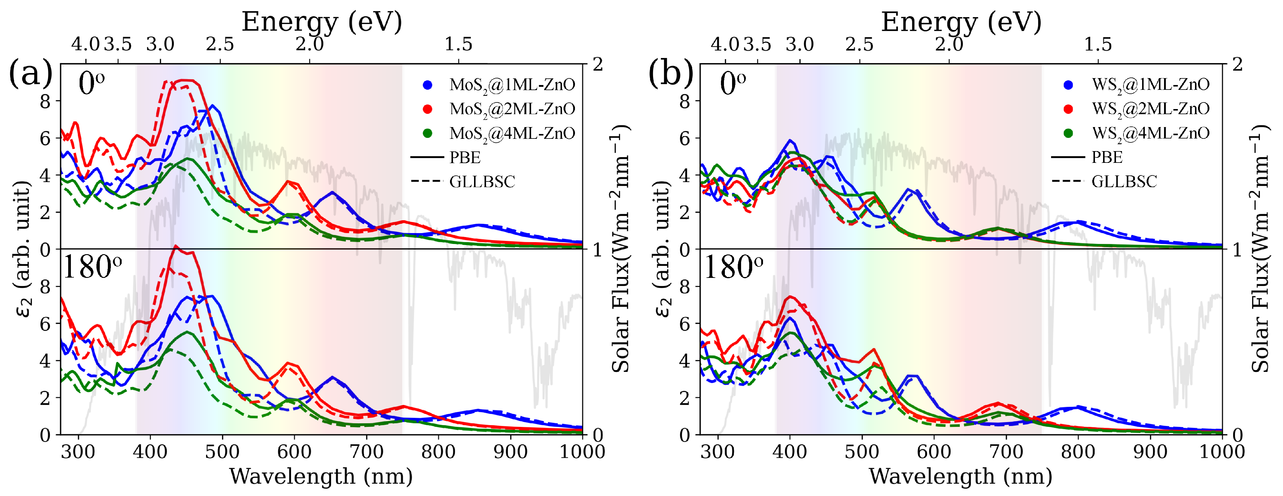
3.3.1. Optical Absorption

The ZnO thin film with deposited XS 2 (X = Mo, W) MLs is expected to significantly overcome the limitation of ZnO materials, revealing the excellent absorption ability for enhancing the application of solar radiation. As the ZnO substrate becomes thicker, the electrons from the substrate are supposed to further boost the absorption. The optical absorption of the MoS 2 @ZnO and WS 2 @ZnO 2D nanocomposites estimated through the calculated ε 2 is shown in Figure 8a,b. To gain more insight into the utilization of solar power, the ε 2 is compared with the solar spectrum [71], helping to analyze the efficiency for photon trapping. At first glance, the MoS 2 and WS 2 actually improve the limited absorption of ZnO substrate in the visible light region. The peak at around 800 nm is due to the underestimation of CBM and band gap. Overall, the ε 2 for MoS 2 @ZnO and WS 2 @ZnO is in agreement with those theoretically predicted previously [25,26,27,29]. For most experiments [2,3,72,73], the obvious enhancement of the first peak at absorption spectrum is around 700 nm. Some of the light-trapping structure of core-shell nanopillar array has a great improvement of absorption at the wavelengths below 800 nm [2]. Although it is hard to derive the real absorption for large-scale MoS 2 @ZnO heterostructure from the atomic-layer simulation, the peak around 800 nm is actually measured in the experiments. In addition, the MoS 2 @ZnO absorption value is normally larger than that measured for WS 2 @ZnO [20,21].
While the feature of g-ZnO substrates becomes the crystal structure (4 layers in 4ML-ZnO), the ε 2 is obviously decreased, especially the wavelengths around 400–500 nm. From the PDOS, the thicker ZnO substrate triggers the increment of O states around VBM. In Figure 7c,d,i,l, there is a strong density of states induced by O states at Γ points. However, the excess of O states does not lead to further improvement of absorption. These results indicate that the crystal-like ZnO substrate with MoS 2 (WS 2 ) composites fails to sustain the strong peak around 400 nm induced in the MoS 2 @g-ZnO and WS 2 @g-ZnO. Although the g-ZnO substrate is constructed for enhancing the absorption, the WS 2 with the rotation angle of 180 does not manifest it in the upper panel of Figure 8b. Despite this, the 1ML-ZnO substrate exhibits the strongest enhancement as compared to 2ML-ZnO and 4ML-ZnO layers in the visible light region.
The enhancement in the absorption implemented due to formations of nanocomposites (2ML-ZnO with TMDs) is compared with photoabsorption calculated for ZnO bulk and free-standing TMD layers in Figure 8. It is worth mentioning that the ε 2 calculated for the layered ZnO substrates and TMD MLs without taking into account the excitonic effect is almost zero around the visible light region in Figure 3b and Figure 5, whereas the ε 2 shown in Figure 8 and Figure 9a calculated without BSE present the obvious peaks related to the ε 2 of TMDs ML calculated with excitonic effect in Figure 5. Due to the extreme weight difference without illustrating the log scale of projected band structures in Figure 9b,c, the contributions for the p 1 and p 2 of ZnO substrates are straightforwardly overlooked around the VBM. The ZnO substrates of 2D nanocomposites actually act as the electrons supplier for the p 1 and p 2 around the K point. Therefore, the heterostructure inherits the peaks of TMDs monolayers, which are marked in Figure 9a. The combination of ZnO and TMDs cause not only the first peak (p 1 ) to be slightly red-shifted (p 1 ) but also other peaks (p 2 and p 3 ) to be a little blue-shifted (p 2 and p 3 ).
Calculated absorption spectra for WS 2 @ZnO heterostructure (Figure 9a, upper panel) demonstrate qualitative agreement with the experimental photoluminescence spectra (PL) for the core-shell WS 2 @ZnO nanowires measured at 9 K (Figure 10) [22]. Note that photoluminescence spectra is usually red-shifted relative to absorption spectra [74]. Positions of PL spectra of WS 2 @ZnO nanowires at 688 nm, 522 nm, and 426 nm can be correlated with p 1 , p 2 , and p 3 peaks of calculated absorption spectra of WS 2 @ZnO heterostructure; however, the most intensive PL peak at 522 nm can be related to ZnO defect photoluminescence.
On the whole, the heterostructure of MoS 2 @ZnO and WS 2 @ZnO generate the broadband situation in the spectrum, which implies more efficient utilization of the solar spectrum.

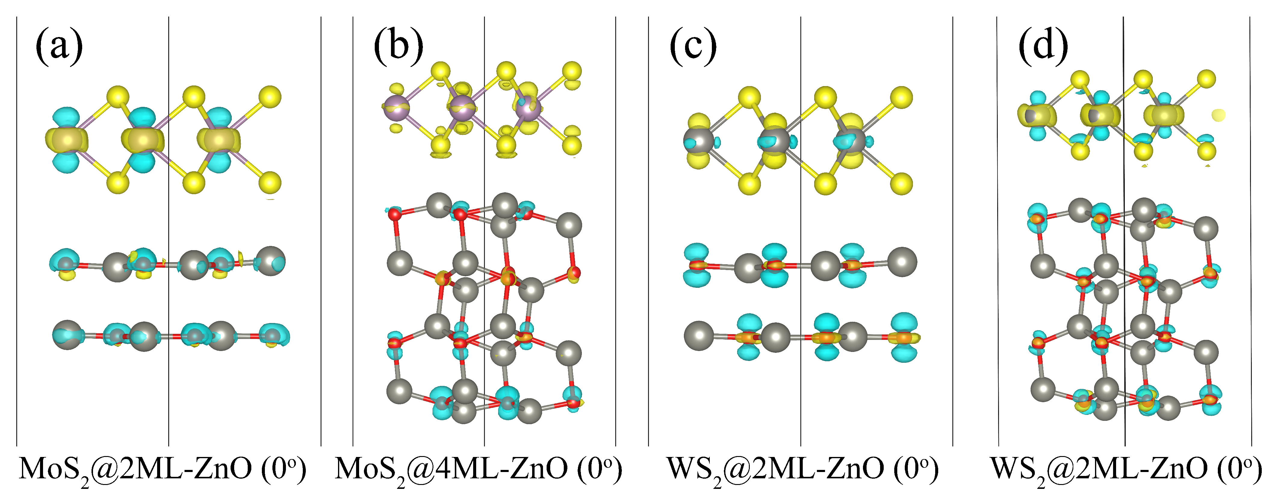
3.3.2. Differential Charge Density Maps

The formation of nanoheterostructure redistributes the total charge density between ZnO substrate and MoS 2 (WS 2 ) MLs, which causes the formation of a built-in electric dipole field at the interface [25,29]. It is hardly possible to estimate the behavior of photogenerated holes and electrons from the ground state calculations. In this study, the excited-state time-independent DFT calculations were performed to obtain the photogenerated charges in comparison with the ground state calculated total charge density. Here, we emphasize that the processes of light-induced electron-hole separation and charge transitions are quite complicated. These processes should include the time-dependent electron-hole interaction, non-adiabatic molecule dynamics, and thermal equilibrium [75,76]. In our simulations, we concentrate only on the response of the orbitals associated with the assigned holes and electrons to mimic the total charge density difference of the interband.
The MoS 2 @ZnO and WS 2 @ZnO with the rotation angle of 0 are selected to provide a deeper understanding of why the bulk-like 4ML-ZnO substrate would lead to the ε 2 decreased at around 400 nm. To construct the differential charge density map, the wave function associated with the CBM was assigned to the occupancy of 1 electron, while the other wave function associated with the CBM at 3.1 eV (400 nm) was assigned to the occupancy of the removed 1 electron. In Figure 11, the difference of total charge density is illustrated. For the ZnO/MoS 2 @2ML-ZnO and WS 2 @2ML-ZnO, the differential charge density accumulates around the Mo and W atoms and depletes at oxygen atoms. This phenomenon reflects the transition behaviors of the O valence states to Mo or W states at the conduction band. Considering the MoS 2 @4ML-ZnO, the the depletion of charge density around the O atoms is observed, while the increase of charge density is not gathered around the Mo atoms. In contrast, the charge density distribution in WS 2 @4ML-ZnO is similar to the WS 2 @2ML-ZnO.

4. Conclusions

Before drawing a conclusion, it should be mentioned that the use of excited-state calculations is necessary for reliable predictions of many processes in solids, including their photocatalytic properties. In this work, the electronic structure and optical properties of MoS 2 and WS 2 monolayers deposited at ZnO and g-ZnO substrates are studied by means of DFT and excited-state time-independent DFT. The electronic structures predicted by means of PBE and GLLBSC exchange-correlation functional differ due to underestimated PBE band gap. The GLLBSC within DFT allows us to estimate the more dense Mo and W states in the vicinity of the VBM. Both PBE and GLLBSC predict a similar imaginary part of the dielectric function. The main conclusion drawn from our theoretical study is that the thicker bulk-like ZnO substrate fails to enhance photoabsorption at MoS 2 @ZnO and WS 2 @ZnO 2D nanocomposites in the visible region of solar spectra, while the graphene-like ZnO substrate can be suggested as the best candidate to improve visible-light-driven photoresponse of nanocomposites under study. MoS 2 and WS 2 single-layered nanofilms are able to strengthen the visible-light-driven photoresponse, even if the bulk-like ZnO substrate is in use. MoS 2 and WS 2 deposited at ZnO produce the absorption peaks of up to 700 nm. Summing up, the 2D nanocomposites made of g-ZnO and TMDs are predicted to exhibit the broadband photoabsorption and can be suggested as an efficient photocatalyst for visible-light-driven water splitting applications.

Author Contributions

Conceptualization, Y.-P.L., B.P., E.B. and S.P.; methodology, Y.-P.L. and S.P.; software, Y.-P.L.; validation, Y.-P.L., B.P., E.B., D.B. and S.P.; formal analysis, Y.-P.L., A.A.P., M.S. and S.P.; investigation, Y.-P.L. and B.P.; resources, S.P.; data curation, Y.-P.L. and S.P.; writing—original draft preparation, Y.-P.L. and S.P.; writing—review and editing, Y.-P.L., B.P., E.B., M.S., D.B. and S.P.; visualization, Y.-P.L. and D.B.; supervision, D.B. and S.P.; project administration, S.P.; funding acquisition, S.P. All authors have read and agreed to the published version of the manuscript.

Funding

This research was funded by the Latvian Scientific Council grant LZP-2018/2-0083. Institute of Solid State Physics, University of Latvia, as the Center of Excellence, has received funding from the European Union’s Horizon 2020 Framework Program H2020-WIDESPREAD-01-2016-2017-TeamingPhase2 under Grant Agreement No. 739508, project CAMART 2 .

Data Availability Statement

The raw/processed data required to reproduce these findings cannot be shared at this time as the data also form a part of an ongoing study.

Acknowledgments

Authors are grateful to K. Smits for photoluminescence spectra measurements of core-shell WS 2 @ZnO nanowires, as well as to A.I. Popov and A. Sternbergs for many stimulating discussion. The calculations were performed at the Latvian SuperCluster (LASC).

Conflicts of Interest

The authors declare no conflict of interest. The funders had no role in the design of the study; in the collection, analysis, or interpretation of data; in the writing of the manuscript, or in the decision to publish the results.

References

  1. Chen, X.; Liu, D.; Gao, Z. Preparation of ZnO Photocatalyst for the Efficient and Rapid Photocatalytic Degradation of Azo Dyes. Nanoscale Res. Lett. 2017, 12, 143. [Google Scholar] [CrossRef] [PubMed] [Green Version]
  2. Ning, L.; Jiang, T.; Shao, Z.; Ding, K.; Zhang, X.; Jie, J. Light-trapping enhanced ZnO-MoS2 core-shell nanopillar arrays for broadband ultraviolet-visible-near infrared photodetection. J. Mater. Chem. C 2018, 6, 7077–7084. [Google Scholar] [CrossRef]
  3. Zhou, Y.H.; Zhang, Z.B.; Xu, P.; Zhang, H.; Wang, B. UV—Visible Photodetector Based on I-type Heterostructure of ZnO-QDs/Monolayer MoS2. Nanoscale Res. Lett. 2019, 14, 364. [Google Scholar] [CrossRef] [Green Version]
  4. Butanovs, E.; Vlassov, S.; Kuzmin, A.; Piskunov, S.; Butikova, J.; Polyakov, B. Fast-Response Single-Nanowire Photodetector Based on ZnO/WS2 Core/Shell Heterostructures. ACS Appl. Mater. Interfaces 2018, 10, 13869–13876. [Google Scholar] [CrossRef]
  5. Gerbreders, V.; Krasovska, M.; Mihailova, I.; Ogurcovs, A.; Sledevskis, E.; Gerbreders, A.; Tamanis, E.; Kokina, I.; Plaksenkova, I. ZnO nanostructure-based electrochemical biosensor for Trichinella DNA detection. Sens. Bio-Sens. Res. 2019, 23, 100276. [Google Scholar] [CrossRef]
  6. Khaliullin, S.M.; Zhuravlev, V.; Ermakova, L.; Buldakova, L.Y.; Yanchenko, M.Y.; Porotnikova, N. Solution combustion synthesis of ZnO using binary fuel (glycine+ citric acid). Int. J. Self-Propag. High-Temp. 2019, 28, 226–232. [Google Scholar] [CrossRef]
  7. Burlacu, A.; Ursaki, V.; Lincot, D.; Skuratov, V.; Pauporte, T.; Rusu, E.; Tiginyanu, I. Enhanced radiation hardness of ZnO nanorods versus bulk layers. Phys. Status Solidi Rapid Res. Lett. 2008, 2, 68–70. [Google Scholar] [CrossRef]
  8. Uklein, A.; Multian, V.; Kuz’micheva, G.; Linnik, R.; Lisnyak, V.; Popov, A.; Gayvoronsky, V.Y. Nonlinear optical response of bulk ZnO crystals with different content of intrinsic defects. Opt. Mater. 2018, 84, 738–747. [Google Scholar] [CrossRef]
  9. Giniyatova, S.; Dauletbekova, A.; Baimukhanov, Z.; Vlasukova, L.; Akilbekov, A.; Usseinov, A.; Kozlovskiy, A.; Akylbekov, A.; Seitbayev, A.; Karipbayev, Z. Structure, electrical properties and luminescence of ZnO nanocrystals deposited in SiO2/Si track templates. Radiat. Meas. 2019, 125, 52–56. [Google Scholar] [CrossRef]
  10. Ostanina, T.; Rudoi, V.; Nikitin, V.; Darintseva, A.; Zalesova, O.; Porotnikova, N. Determination of the surface of dendritic electrolytic zinc powders and evaluation of its fractal dimension. Russ. J. Non-Ferr. Met. 2016, 57, 47–51. [Google Scholar] [CrossRef]
  11. Krasovska, M.; Gerbreders, V.; Tamanis, E.; Gerbreders, S.; Bulanovs, A. The study of adsorption process of Pb ions using well-aligned arrays of ZnO nanotubes as a sorbent. Latv. J. Phys. Tech. Sci. 2017, 54, 41. [Google Scholar] [CrossRef] [Green Version]
  12. Dauletbekova, A.; Kozlovskyi, A.; Akilbekov, A.; Seitbayev, A.; Alzhanova, A. Synthesis of ZnO nanocrystals in a-SiO2/Si ion track templates. Surf. Coat. Technol. 2018, 355, 11–15. [Google Scholar] [CrossRef]
  13. Pankratov, V.; Osinniy, V.; Larsen, A.N.; Nielsen, B.B. ZnO nanocrystals/SiO2 multilayer structures fabricated by RF-magnetron sputtering. Phys. B Condens. Matter. 2009, 404, 4827–4830. [Google Scholar] [CrossRef]
  14. Latronico, G.; Singh, S.; Mele, P.; Darwish, A.; Sarkisov, S.; Pan, S.W.; Kawamura, Y.; Sekine, C.; Baba, T.; Mori, T.; et al. Synthesis and characterization of Al-and SnO2-doped ZnO thermoelectric thin films. Materials 2021, 14, 6929. [Google Scholar] [CrossRef] [PubMed]
  15. Biswas, S.; Singh, S.; Singh, S.; Chattopadhyay, S.; De Silva, K.K.H.; Yoshimura, M.; Mitra, J.; Kamble, V.B. Selective Enhancement in Phonon Scattering Leads to a High Thermoelectric Figure-of-Merit in Graphene Oxide-Encapsulated ZnO Nanocomposites. ACS Appl. Mater. Interfaces 2021, 13, 23771–23786. [Google Scholar] [CrossRef] [PubMed]
  16. Harun, K.; Salleh, N.; Bahri, D.; Yaakob, M.; Mohamad, A.A. DFT+U calculations for electronic, structural, and optical properties of ZnO wurtzite structure: A Review. Results Phys. 2019, 16, 102829. [Google Scholar] [CrossRef]
  17. Yoshikawa, H.; Adachi, S. Optical Constants of ZnO. Jpn. J. Appl. Phys. 1997, 36, 6237–6243. [Google Scholar] [CrossRef]
  18. Wibowo, A.; Marsudi, M.A.; Amal, M.I.; Ananda, M.B.; Stephanie, R.; Ardy, H.; Diguna, L.J. ZnO nanostructured materials for emerging solar cell applications. RSC Adv. 2020, 10, 42838–42859. [Google Scholar] [CrossRef]
  19. Farh, H.; Noua, A.; Guemini, R.; Guitoume, D.E.; Zaoui, O. Thickness Effect of ZnO Film on the Performance of Photocatalytic in a p-NiO/n-ZnO Heterostructure under Solar Light Irradiation. J. Nano Res. 2020, 62, 87–95. [Google Scholar] [CrossRef]
  20. Mishra, A.; Lakshmi, K.; Huang, L. Eco-friendly synthesis of metal dichalcogenides nanosheets and their environmental remediation potential driven by visible light. Sci. Rep. 2015, 5, 15718. [Google Scholar] [CrossRef] [Green Version]
  21. Dong, N.; Li, Y.; Feng, Y.; Zhang, S.; Zhang, X.; Chang, C.; Fan, J.; Zhang, L.; Wang, J. Optical Limiting and Theoretical Modelling of Layered Transition Metal Dichalcogenide Nanosheets. Sci. Rep. 2015, 5, 14646. [Google Scholar] [CrossRef] [Green Version]
  22. Polyakov, B.; Kuzmin, A.; Smits, K.; Zideluns, J.; Butanovs, E.; Butikova, J.; Vlassov, S.; Piskunov, S.; Zhukovskii, Y.F. Unexpected Epitaxial Growth of a Few WS2 Layers on 1100 Facets of ZnO Nanowires. J. Phys. Chem. C 2016, 120, 21451–21459. [Google Scholar] [CrossRef]
  23. Butanovs, E.; Kuzmin, A.; Butikova, J.; Vlassov, S.; Polyakov, B. Synthesis and characterization of ZnO/ZnS/MoS2 core-shell nanowires. J. Cryst. Growth 2017, 459, 100–104. [Google Scholar] [CrossRef]
  24. Kim, M.S.; Roy, S.; Lee, J.; Kim, B.; Kim, H.; Park, J.H.; Yun, S.; Han, G.; Leem, J.Y.; Kim, J. Enhanced Light Emission from Monolayer Semiconductors by Forming Heterostructures with ZnO Thin Films. ACS Appl. Mater. Interfaces 2016, 8, 28809–28815. [Google Scholar] [CrossRef] [PubMed]
  25. Wang, S.; Tian, H.; Ren, C.; Yu, J.; Sun, M. Electronic and optical properties of heterostructures based on transition metal dichalcogenides and graphene-like zinc oxide. Sci. Rep. 2018, 8, 12009. [Google Scholar] [CrossRef] [PubMed]
  26. Wang, G.; Li, D.; Sun, Q.; Dang, S.; Zhong, M.; Xiao, S.; Liu, G. Hybrid Density Functional Study on the Photocatalytic Properties of Two-dimensional g-ZnO Based Heterostructures. Nanomaterials 2018, 8, 374. [Google Scholar] [CrossRef] [Green Version]
  27. Wang, G.; Yuan, H.; Chang, J.; Wang, B.; Kuang, A.; Chen, H. ZnO/MoX2 (X = S, Se) composites used for visible light photocatalysis. RSC Adv. 2018, 8, 10828–10835. [Google Scholar] [CrossRef] [Green Version]
  28. Usseinov, A.; Akilbekov, A.; Kotomin, E.; Popov, A.; Seitov, D.; Nekrasov, K.; Giniyatova, S.G.; Karipbayev, Z.T. The first principles calculations of CO2 adsorption on (1010) ZnO surface. AIP Conf. Proc. 2019, 2174, 020181. [Google Scholar] [CrossRef]
  29. Wang, S.; Ren, C.; Tian, H.; Yu, J.; Sun, M. MoS2/ZnO van der Waals heterostructure as a high-efficiency water splitting photocatalyst: A first-principles study. Phys. Chem. Chem. Phys. 2018, 20, 13394–13399. [Google Scholar] [CrossRef]
  30. Zdeshchyts, A.V.; Balabai, R.M. Electronic Properties of a Hybrid Composite of Nanocellulose/Graphene-Like ZnO from Calculations on the Basis of the First Principles. Nanosistemi Nanomater. Nanotehnologii 2019, 17, 283–298. [Google Scholar] [CrossRef]
  31. Theerthagiri, J.; Chandrasekaran, S.; Salla, S.; Elakkiya, V.; Senthil, R.; Nithyadharseni, P.; Maiyalagan, T.; Micheal, K.; Ayeshamariam, A.; Arasu, M.V.; et al. Recent developments of metal oxide based heterostructures for photocatalytic applications towards environmental remediation. J. Solid State Chem. 2018, 267, 35–52. [Google Scholar] [CrossRef]
  32. Putritama, V.; Fauzia, V.; Supangat, A. The effect of the layer number of MoS2 nanosheets on the photocatalytic efficiency of ZnO/MoS2. Surf. Interfaces. 2020, 21, 100745. [Google Scholar] [CrossRef]
  33. Catlow, R.; Guo, Z.X.; Miskufova, M.; Shevlin, S.; Smith, A.; Sokol, A.; Walsh, A.; Wilson, D.; Woodley, S. Advances in Computational Studies of Energy Materials. Phil. Trans. R. Soc. A 2010, 368, 3379–3456. [Google Scholar] [CrossRef] [Green Version]
  34. Puchin, V.E.; Shluger, A.L.; Itoh, N. Theoretical studies of atomic emission and defect formation by electronic excitation at the (100) surface of NaCl. Phys. Rev. B 1993, 47, 10760–10768. [Google Scholar] [CrossRef]
  35. Emeline, A.V.; Kataeva, G.V.; Ryabchuk, V.K.; Serpone, N. Photostimulated Generation of Defects and Surface Reactions on a Series of Wide Band Gap Metal-Oxide Solids. J. Phys. Chem. B 1999, 103, 9190–9199. [Google Scholar] [CrossRef]
  36. Monge, M.A.; González, R.; Muñoz Santiuste, J.E.; Pareja, R.; Chen, Y.; Kotomin, E.A.; Popov, A.I. Photoconversion and dynamic hole recycling process in anion vacancies in neutron-irradiated MgO crystals. Phys. Rev. B 1999, 60, 3787–3791. [Google Scholar] [CrossRef]
  37. Monge, M.; González, R.; Muñoz Santiuste, J.; Pareja, R.; Chen, Y.; Kotomin, E.; Popov, A. Photoconversion of F+ centers in neutron-irradiated MgO. Nucl. Instrum. Methods Phys. Res. 2000, 166–167, 220–224. [Google Scholar] [CrossRef]
  38. Chernov, S.A.; Trinkler, L.; Popov, A.I. Photo- and thermo-stimulated luminescence of CsI—Tl crystal after UV light irradiation at 80 K. Radiat. Eff. Defects Solids 1998, 143, 345–355. [Google Scholar] [CrossRef]
  39. Sterrer, M.; Diwald, O.; Knözinger, E.; Sushko, P.V.; Shluger, A.L. Energies and Dynamics of Photoinduced Electron and Hole Processes on MgO Powders. J. Phys. Chem. 2002, 106, 12478–12482. [Google Scholar] [CrossRef]
  40. Karmakar, K.; Maity, D.; Pal, D.; Mandal, K.; Khan, G.G. Photo-Induced Exciton Dynamics and Broadband Light Harvesting in ZnO Nanorod-Templated Multilayered Two-Dimensional MoS2/MoO3 Photoanodes for Solar Fuel Generation. ACS Appl. Nano Mater. 2020, 3, 1223–1231. [Google Scholar] [CrossRef]
  41. Wu, H.; Wang, M.; Huai, L.; Wang, W.; Zhang, J.; Wang, Y. Optical storage and operation based on photostimulated luminescence. Nano Energy 2021, 90, 106546. [Google Scholar] [CrossRef]
  42. Yuan, L.; Jin, Y.; Su, Y.; Wu, H.; Hu, Y.; Yang, S. Optically Stimulated Luminescence Phosphors: Principles, Applications, and Prospects. Laser Photonics Rev. 2020, 14, 2000123. [Google Scholar] [CrossRef]
  43. Claeyssens, F.; Freeman, C.L.; Allan, N.L.; Sun, Y.; Ashfold, M.N.R.; Harding, J.H. Growth of ZnO thin films—Experiment and theory. J. Mater. Chem. 2005, 15, 139–148. [Google Scholar] [CrossRef]
  44. Tusche, C.; Meyerheim, H.L.; Kirschner, J. Observation of Depolarized ZnO(0001) Monolayers: Formation of Unreconstructed Planar Sheets. Phys. Rev. Lett. 2007, 99, 026102. [Google Scholar] [CrossRef] [PubMed] [Green Version]
  45. Ta, H.Q.; Zhao, L.; Pohl, D.; Pang, J.; Trzebicka, B.; Rellinghaus, B.; Pribat, D.; Gemming, T.; Liu, Z.; Bachmatiuk, A.; et al. Graphene-Like ZnO: A Mini Review. Crystals 2016, 6, 100. [Google Scholar] [CrossRef] [Green Version]
  46. Mortensen, J.J.; Hansen, L.B.; Jacobsen, K.W. Real-space grid implementation of the projector augmented wave method. Phys. Rev. B 2005, 71, 035109. [Google Scholar] [CrossRef] [Green Version]
  47. Enkovaara, J.; Rostgaard, C.; Mortensen, J.J.; Chen, J.; Dułak, M.; Ferrighi, L.; Gavnholt, J.; Glinsvad, C.; Haikola, V.; Hansen, H.A.; et al. Electronic structure calculations with GPAW: A real-space implementation of the projector augmented-wave method. J. Condens. Matter Phys. 2010, 22, 253202. [Google Scholar] [CrossRef]
  48. Larsen, A.H.; Mortensen, J.J.; Blomqvist, J.; Castelli, I.E.; Christensen, R.; Duaak, M.; Friis, J.; Groves, M.N.; Hammer, B.; Hargus, C.; et al. The atomic simulation environment – Python library for working with atoms. J. Condens. Matter Phys. 2017, 29, 273002. [Google Scholar] [CrossRef] [Green Version]
  49. Bahn, S.R.; Jacobsen, K.W. An object-oriented scripting interface to a legacy electronic structure code. Comput. Sci. Eng. 2002, 4, 56–66. [Google Scholar] [CrossRef] [Green Version]
  50. Perdew, J.P.; Burke, K.; Ernzerhof, M. Generalized Gradient Approximation Made Simple. Phys. Rev. Lett. 1996, 77, 3865–3868. [Google Scholar] [CrossRef] [Green Version]
  51. Grimme, S.; Antony, J.; Ehrlich, S.; Krieg, H. A Consistent and Accurate Ab Initio Parametrization of Density Functional Dispersion Correction (DFT-D) for the 94 Elements H-Pu. J. Chem. Phys. 2010, 132, 154104. [Google Scholar] [CrossRef] [Green Version]
  52. Kuisma, M.; Ojanen, J.; Enkovaara, J.; Rantala, T.T. Kohn-Sham potential with discontinuity for band gap materials. Phys. Rev. B 2010, 82, 115106. [Google Scholar] [CrossRef] [Green Version]
  53. Anisimov, V.I.; Zaanen, J.; Andersen, O.K. Band theory and Mott insulators: Hubbard U instead of Stoner I. Phys. Rev. B 1991, 44, 943–954. [Google Scholar] [CrossRef] [PubMed] [Green Version]
  54. Ma, X.; Wu, Y.; Lv, Y.; Zhu, Y. Correlation Effects on Lattice Relaxation and Electronic Structure of ZnO within the GGA+U Formalism. J. Phys. Chem. C 2013, 117, 26029–26039. [Google Scholar] [CrossRef]
  55. Guan, Y.; Yao, H.; Zhan, H.; Wang, H.; Zhou, Y.; Kang, J. Optoelectronic properties and strain regulation of the 2D WS2/ZnO Van der Waals heterostructure. RSC Adv. 2021, 11, 14085–14092. [Google Scholar] [CrossRef]
  56. Yan, J.; Mortensen, J.J.; Jacobsen, K.W.; Thygesen, K.S. Linear density response function in the projector augmented wave method: Applications to solids, surfaces, and interfaces. Phys. Rev. B 2011, 83, 245122. [Google Scholar] [CrossRef] [Green Version]
  57. Hüser, F.; Olsen, T.; Thygesen, K.S. How dielectric screening in two-dimensional crystals affects the convergence of excited-state calculations: Monolayer MoS2. Phys. Rev. B 2013, 88, 245309. [Google Scholar] [CrossRef] [Green Version]
  58. Olsen, T.; Latini, S.; Rasmussen, F.; Thygesen, K.S. Simple Screened Hydrogen Model of Excitons in Two-Dimensional Materials. Phys. Rev. Lett. 2016, 116, 056401. [Google Scholar] [CrossRef] [Green Version]
  59. Barca, G.M.J.; Gilbert, A.T.B.; Gill, P.M.W. Simple Models for Difficult Electronic Excitations. J. Chem. Theory Comput. 2018, 14, 1501–1509. [Google Scholar] [CrossRef]
  60. Ivanov, A.V.; Levi, G.; Jansson, E.A.; Jansson, H. Method for Calculating Excited Electronic States Using Density Functionals and Direct Orbital Optimization with Real Space Grid or Plane-Wave Basis Set. J. Chem. Theory Comput. 2021, 17, 5034–5049. [Google Scholar] [CrossRef]
  61. Dong, X.; Mahler, A.D.; Kempfer-Robertson, E.M.; Thompson, L.M. Global Elucidation of Self-Consistent Field Solution Space Using Basin Hopping. J. Chem. Theory Comput. 2020, 16, 5635–5644. [Google Scholar] [CrossRef]
  62. Momma, K.; Izumi, F. VESTA 3 for three-dimensional visualization of crystal, volumetric and morphology data. J. Appl. Cryst 2011, 44, 1272–1276. [Google Scholar] [CrossRef]
  63. Van der Walt, S.; Colbert, S.C.; Varoquaux, G. The numpy array: A structure for efficient numerical computation. Comput. Sci. Eng. 2011, 13, 22–30. [Google Scholar] [CrossRef] [Green Version]
  64. Hunter, J.D. Matplotlib: A 2D graphics environment. Comput. Sci. Eng. 2007, 9, 90–95. [Google Scholar] [CrossRef]
  65. Hong, H.K.; Jo, J.; Hwang, D.; Lee, J.; Kim, N.Y.; Son, S.; Kim, J.H.; Jin, M.J.; Jun, Y.C.; Erni, R.; et al. Atomic scale study on growth and heteroepitaxy of ZnO monolayer on graphene. Nano lett. 2017, 17, 120–127. [Google Scholar] [CrossRef] [PubMed] [Green Version]
  66. Özgür, Ü.; Alivov, Y.I.; Liu, C.; Teke, A.; Reshchikov, M.; Doğan, S.; Avrutin, V.; Cho, S.J.; Morkoç, H. A comprehensive review of ZnO materials and devices. J. Appl. Phys. 2005, 98, 041301. [Google Scholar] [CrossRef] [Green Version]
  67. Topsakal, M.; Cahangirov, S.; Bekaroglu, E.; Ciraci, S. First-principles study of zinc oxide honeycomb structures. Phys. Rev. B 2009, 80, 235119. [Google Scholar] [CrossRef] [Green Version]
  68. Li, X.D.; Chen, T.; Liu, P.; Liu, Y.; Liu, Z.; Leong, K. A study on the evolution of dielectric function of ZnO thin films with decreasing film thickness. J. Appl. Phys. 2014, 115, 103512. [Google Scholar] [CrossRef]
  69. Pesic, J.; Vujin, J.; Tomasevic-Ilic, T.; Spasenovic, M.; Gajic, R. DFT study of optical properties of MoS2 and WS2 compared to spectroscopic results on liquid phase exfoliated nanoflakes. Opt. Quantum Electron. 2018, 50, 291. [Google Scholar] [CrossRef]
  70. Li, Y.; Chernikov, A.; Zhang, X.; Rigosi, A.; Hill, H.M.; van der Zande, A.M.; Chenet, D.A.; Shih, E.M.; Hone, J.; Heinz, T.F. Measurement of the optical dielectric function of monolayer transition-metal dichalcogenides: MoS2, MoSe2, WS2, and WSe2. Phys. Rev. B 2014, 90, 205422. [Google Scholar] [CrossRef] [Green Version]
  71. The AM1.5G Spectrum Was Taken from the NREL. Available online: http://rredc.nrel.gov/solar/spectra/am1.5 (accessed on 27 December 2021).
  72. Yuan, Y.J.; Lu, H.; Wang, F.; Hu, B.; Yu, Z.T.; Zou, Z. Significant Enhancement in Photocatalytic Hydrogen Evolution from Water by MoS2 Nanosheet-coated ZnO Heterostructure Photocatalyst. Dalton Trans. 2015, 44, 10997–11003. [Google Scholar] [CrossRef] [PubMed]
  73. Lan, C.; Li, C.; Wang, S.; Yin, Y.; Guo, H.; Liu, N.; Liu, Y. ZnO-WS2 heterostructures for enhanced ultra-violet photodetectors. RSC Adv. 2016, 6, 67520–67524. [Google Scholar] [CrossRef]
  74. Krasnok, A.; Lepeshov, S.; Alú, A. Nanophotonics with 2D transition metal dichalcogenides. Opt. Express 2018, 26, 15972–15994. [Google Scholar] [CrossRef] [PubMed] [Green Version]
  75. Tritsaris, G.A.; Vinichenko, D.; Kolesov, G.; Friend, C.M.; Kaxiras, E. Dynamics of the Photogenerated Hole at the Rutile TiO2(110)/Water Interface: A Nonadiabatic Simulation Study. J. Phys. Chem. C 2014, 118, 27393–27401. [Google Scholar] [CrossRef]
  76. Kolesov, G.; Vinichenko, D.; Tritsaris, G.A.; Friend, C.M.; Kaxiras, E. Anatomy of the Photochemical Reaction: Excited-State Dynamics Reveals the C-H Acidity Mechanism of Methoxy Photo-oxidation on Titania. J. Phys. Chem. Lett. 2015, 6, 1624–1627. [Google Scholar] [CrossRef] [PubMed]
Figure 1. Top view (a) and side view (b) of the models of MoS 2 @ZnO and WS 2 @ZnO nanocomposites with graphene-like 1ML-ZnO and 2ML-ZnO substrates, as well as the wurtzite-like 4ML-ZnO substrate. Structures with 0 and 180 rotation angles are shown. Inset tables list the average bond lengths in Å.
Energies 15 00150 g001
Figure 2. Schematic representation of non-distorted and equilibrium atomic structure of layered ZnO substrates. The definition of wurtzute-like Zn–O interlayer bond length d’ Z n O is based on prescriptions given by Tusche et al. [44].
Energies 15 00150 g002
Figure 3. Band gap (a) and imaginary part of dielectric function ( ε 2 ) (b) of 1ML-, 2ML-, and 4ML-ZnO substrates calculated by means of PBE and GLLBSC E X C s. The upper panel in (b) shows ε 2 calculated by means of PBE E X C , while the bottom panel shows ε 2 calculated by means of GLLBSC E X C . The experimental ε 2 graph of bulk ZnO has been reported by Yoshikawa and Adachi elsewhere [17].
Energies 15 00150 g003
Figure 4. Band structures and projected density of states (PDOS) as calculated for (a) MoS 2 and (b) WS 2 monolayers.
Energies 15 00150 g004
Figure 5. Imaginary part of dielectric function ( ε 2 ) as calculated for MoS 2 (purple) and WS 2 (yellow) monolayers by means of GLLBSC E X C .
Energies 15 00150 g005
Figure 6. Band edge positions of (a) MoS 2 @ZnO and (b) WS 2 @ZnO 2D nanocomposites as calculated by means of PBE E X C (red) and GLLBSC E X C (blue) with respect to the water splitting redox levels. The light and dark colors stand for the TMD/ZnO rotation angles of 0 and 180 , respectively.
Energies 15 00150 g006
Figure 7. Band structures and projected density of states (PDOS) as calculated for MoS 2 (af) and WS 2 (gl) deposited at 1ML-, 2ML-, and 4ML-ZnO substrates. Odd rows show the MoS 2 @ZnO (WS 2 @ZnO) with the rotation angle of 0 , while even rows indicate the MoS 2 @ZnO (WS 2 @ZnO) at 180 . The insets show the atomic structures of MoS 2 @ZnO and WS 2 @ZnO 2D nanocomposites.
Energies 15 00150 g007
Figure 8. Imaginary part of dielectric function ( ε 2 ) of the MoS 2 @ZnO (a) and WS 2 @ZnO (b) 2D nanocomposites. The upper and lower panels are for the MoS 2 and WS 2 with the rotation angle of 0 and 180 , respectively. The right y-axis stands for the solar spectrum based on AM 1.5 [71] (gray curve).
Energies 15 00150 g008
Figure 9. Enhancement of imaginary part of dielectric function ( ε 2 ) in comparison with free-standing ZnO and TMDs MLs (a) and the projected band structures of MoS 2 @2ML-ZnO (b) and WS 2 @2ML-ZnO (c) as calculated by means of GLLBSC E X C . The upper and bottom panels in (a) show the MoS 2 @2ML-ZnO and WS 2 @2ML-ZnO, respectively, with the rotation angle of 180 . The ε 2 of ZnO bulk and TMD MLs are the same as shown in Figure 3 and Figure 5. The insets in (b,c) indicate the log-scale of projected band contributions for TMDs MLs and 2ML-ZnO substrates around VBM and CBM.
Energies 15 00150 g009
Figure 10. Comparison of the photoluminescence (PL) spectra measured for WS 2 @ZnO nanowire at 9 K using the fourth harmonic (266 nm, or 4.66 eV) of a Nd:YAG laser FQSS266 (CryLas GmbH) as an excitation source (green solid line) and calculated absorption spectra for WS 2 @ZnO heterostructure with the rotation angle of 180 (magenta line). The photoluminescence spectra were recorded using the Andor Shamrock B-303i spectrograph equipped with a CCD camera (Andor DU-401A-BV). Spectrum of ZnO nanowires measured at room temperature is drawn with black dotted line [22].
Energies 15 00150 g010
Figure 11. Side views of the differential total charge density maps calculated for MoS 2 @ZnO (a,b) and WS 2 @ZnO (c,d). The yellow and cyan colors indicate accumulated and depleted charge density, respectively. The isosurface increment value is 0.01 bohr 3 .
Energies 15 00150 g011
Publisher’s Note: MDPI stays neutral with regard to jurisdictional claims in published maps and institutional affiliations.

